- On March 28, 2025
- In blog
3 Points to Know BGA: Features Soldering and X-ray Inspection
Nowadays, electronic products are getting thinner and smaller, but more and more powerful. There is a key role behind this: BGA packaging technology.
When a chip needs to be crammed with hundreds of interfaces and compressed to its maximum size, traditional packages are no longer able to do so. BGA makes it easy to realize BGA ICs with 500 IOs by using miniature solder balls neatly arranged at the bottom of the chip, which makes it possible to design and manufacture compact products.
BGA technology is ubiquitous, from 5G base stations to smart watches. In this article, we discuss the following,
- Featuresof BGA: What are the advantages of BGA? What are its types?
- Soldering technology of BGA: How is BGA soldered to PCB?
- Inspection Technology of BGA: Why BGA can only be inspected by X-ray Inspection?
Features of BGA
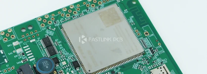
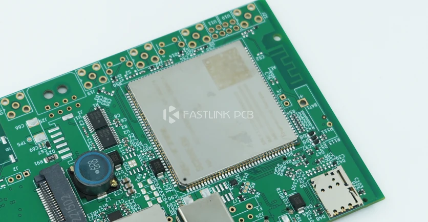
A Ball Grid Array (BGA) is an SMD component without leads. Whereas conventional chips stand on pins sticking out from the perimeter, it is straightforward to “grow” the entire bottom surface full of solder balls – little metal balls that act as miniature piers to hold the chip steady on the board. Even better, these solder balls in the bottom of the chip in a neat square formation. This design allows more connections to be made in the same area.
Advantages and Disadvantages of BGA

Advantages of BGA
- Saving space
- Strong electrical performance
- High heat dissipation
- Easier soldering
- Low cost
Disadvantages of BGA
- Difficult to inspect after soldering.
- Difficult to rework and repair
- Requires electrostatic protection
- High requirements for storage environment
Types of BGA
1.Ceramic BGA (CBGA)
Features: Ceramic substrate with solder containing 10% tin and 90% lead. The melting point is extremely high, so the C4 method (Controlled Folded Chip Attachment) is required to bridge the BGA and PCB.
Advantages: Strong heat dissipation, stable conductivity, suitable for high performance devices.
Applications: Telecommunications and high performance computing.
2.Plastic Laminate BGA (PBGA)
Features: The most mainstream double-sided PCB package, the core material is high-temperature resistant BT resin, coupled with overmolded pad array carrier (OMPAC) sealant technology or solder ball to pad array carrier (GTPAC).
Benefits: Cost effective, supports 200-500 solder ball arrays.
Applications: Consumer appliances and medium power communication technologies.
3.Tape BGA (TBGA)
Features: Utilizes a flexible tape substrate instead of the traditional rigid laminate.
Advantages: Strong heat dissipation, thinner and lighter package
Applications: Portable and high performance electronic devices
4.PoP Package
Features: Vertically stacked like building blocks, each IC has its own BGA, supports individual replacement of damaged parts
Advantages: Can meet the needs of fine pitch, small size, high speed and small installation space.
Applications: Electronics such as smart phones and digital cameras.
5.Contact Array Package (LGA)
Features: Replaces traditional pins with metal pads (“lands”), which are usually organized into a grid or array at the bottom of the package.
Advantages: Supports 8-1681 contacts, suitable for high-density I/O requirements
Applications: Industrial automation, medical equipment and other high-reliability demanding scenarios
Soldering Techniques for BGA

●BGA Storage Conditions:
BGA components, as humidity sensitive components, must be stored in a constant temperature, dry environment. Ideal storage conditions are a temperature of 20-25°C and a humidity of about 10%, preferably protected by nitrogen.
●BGA Pre-treatment:
In order to prevent moisture effects, BGAs need to be baked before soldering at a temperature that should not exceed 125°C to avoid changes in the metal structure. During the soldering process, take care that the temperature is not too high, as this may lead to the separation of the solder ball from the package, affecting the quality of the solder. While the temperature is too low to effectively remove moisture. It is important to note that after baking, the BGA needs to be cooled for about half an hour.
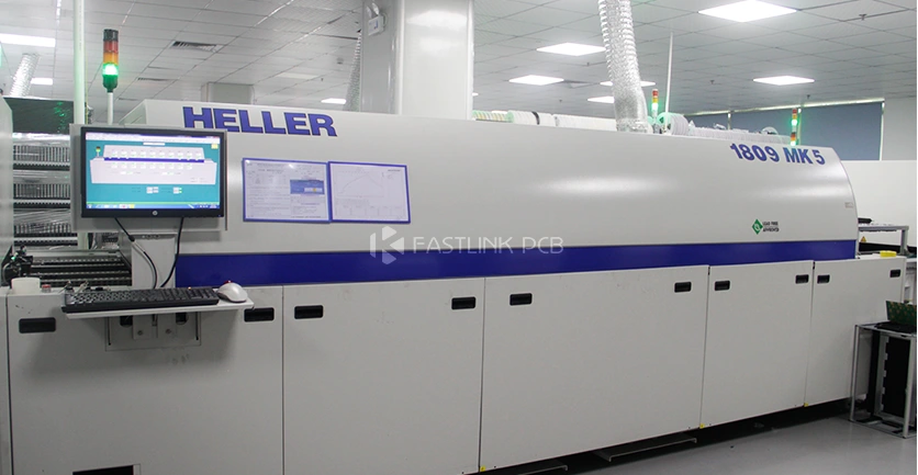
●BGA Reflow Soldering:
1.Preheating zone: PCB temperature should be steadily increased, the rate is controlled within 2°C/s, and the time is controlled at 60-90 seconds. This can stabilize the activation of flux to prevent PCB deformation due to excessive heating.
2.Heat soak zone: the temperature is maintained at 150-180 ° C for 60-120 seconds to evaporate the flux, the rate of heating should be 0.3-0.5 ° C / s.
3.Reflow zone: Temperature over 183°C for 60-90 seconds to ensure that the solder paste melts into a liquid.
4.Cooling zone: solder paste solidifies, components are fixed, temperature drop should be controlled within 3°C/s to avoid PCB deformation.
Inspection Technology for BGA
As we all know, BGAs cannot be inspected by AOI technology, this is because the solder joints are located underneath the BGAs and we cannot see them. The electrical test can only reflect the conductivity of BGA at a specific moment, and cannot predict the long-term stability of the solder joints. For this reason, X-ray inspection has become an effective means of inspecting BGA solder joints. x-ray inspection can be categorized into transmission inspection and cross-section inspection.
1.X-Ray Transmission Inspection
This is a common BGA inspection method, which can detect most of the defects of solder joints through BGA components. However, it is difficult to recognize defects with insufficient solder. Because the solder ball may block the formation of solder image. For example, ceramic BGA will generate eutectic solder, this eutectic solder will be covered by the solder ball, resulting in undetectable.
2.X-ray Cross-section
X-ray cross-section is a layered scanning of solder joints, which makes up for the shortcomings of X-ray transmission inspection. It can also detect the thickness of the ring at the level of the soldering station to analyze the solder reflow process or the change of solder at the soldering site. The radius of the solder ball is detected to analyze the coplanarity between solder joints or between boards.
BGA PCB Assembly Service Provided by Fastlink
BGA package has become the core support for miniaturization of modern electronic devices due to its high-density layout, stable heat dissipation performance and reliable soldering process.Fastlink has been deeply engaged in high-density PCB manufacturing for more than ten years. With fully automated placement lines and multi-million level X-ray inspection systems, we provide our global customers with:
- All types of BGA assembly services
- Soldering of ultra-fine pitch BGAs down to 0.3mm.
- X-ray transmission + X-ray cross-section inspection
- 72 hours very fast prototyping
If you still have any questions about BGA or want to know how much your BGA PCB cost? Welcome to contact us in the lower right corner, we will give you the price within 24h.