- On November 19, 2024
- In blog
8 Types of Vias on a PCB: Design Details You Need to Know
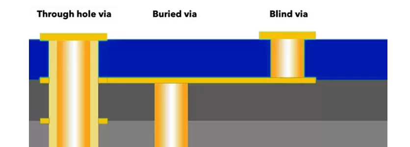
Holes in PCB help us with circuit connection, signal transmission and space optimisation. Different types of holes provide designers with a variety of way to do this, but they also differ in their design characteristics. In the next section, we will introduce the eight major PCB hole type to help you better optimise your design, improve PCB reliability and effectively control manufacturing costs in real PCB projects.
1.Through-Hole Vias
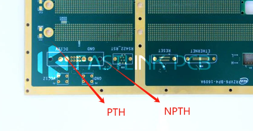
The most common and simplest type of PCB via are through hole. They run the entire length of the PCB, from the top layer all the way down to the bottom layer. If you hold the PCB up to the light, the light can pass right through the hole.
Through-hole can be divided into two types: PTH (plated through-holes) and NPTH (non-plated through-holes). The difference lie in the copper plating on the inside of the hole. PTH is mainly used for connecting and conducting wiring between different layer in a PCB or as component hole for soldering DIP component. NPTH is non-conductive and is usually used for mechanical fixing, e.g. screws or connectors to fasten the PCB to a housing or other structure.
The through-hole also serve as a thermal conduction channel to help conduct heat from one side of the PCB to the other, effectively improving the PCB’s thermal performance. It also facilitates testing and rework, as the through-hole can be accessed from both side of the PCB. However, because the through hole run through all layer and has a relatively large diameter, it take up wiring space on each layer, which can be a limiting factor in HDI PCB design. In high frequency circuit, via may also introduce parasitic inductance and capacitance that can affect signal integrity.
Therefore, if certain connections do not need to run through all layers of the board, designer can choose other types of via, such as blind or buried via, to save space and increase the density of the PCB layout.
2. Blind Vias
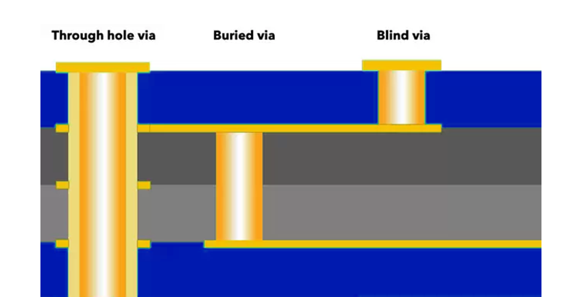
Blind via are commonly used in BGA assembly and HDI PCB. It is a hole that is drilled from the surface layer (top or bottom) of the PCB to the inner layer and plated to create an electrical connection. You can see the blind via on the surface of the PCB, but since it do not go through the entire board, it cannot be seen from the other side. It is mainly used when it is necessary to connect surface mounted component to the inner layer and you don’t want to add too many wiring layer.
The advantage of blind via is that they increase the density of the PCB, making more efficient use of space and reducing the size, number of layer and weight of the PCB, which is particularly beneficial for reducing manufacturing cost and miniaturising equipment. Blind via also reduce EMI and crosstalk, improving signal quality and reliability.
However, there are disadvantage to using blind via. Blind hole fabrication require very precise drilling and plating processes, thus increasing the complexity and cost of fabrication, potentially reducing the number of layers available, and affecting the flexibility of the PCB design.
The challenge of blind hole fabrication are mainly in the need for precise drilling and plating processes, which may increase production cost. When creating blind via, the depth of the drilled holes needs to be precisely defined. Hole that are too shallow may result in poor connection, while hole that are too deep may cause signal distortion or performance degradation. The design must also consider the aspect ratio of the blind hole. An aspect ratio that is too large can make manufacturing more difficult, which in turn lead to more cost and potential production problem.
3. Buried Vias
Unlike blind via, buried via typically connect multiple inner layers of circuitry, rather than a connection between an outer layer and an inner layer. These holes are completely encapsulated inside the board and do not penetrate the outer surface of the board. This feature helps designers make efficient use of limited board space.
Because of the way buried vias are designed, they offer significant advantages, including:
- Enhanced signal integrity: Buried via directly connect different inner layer, shortening the signal transmission path and thus reducing signal delay and reflections, making them ideal for high-speed PCBs.
- Optimised use of space: Optimised use of space: Because the buried via are hidden within the inner layer, they free up surface space on the PCB, allowing for high density component to be placed.
- Enhanced EMI performance: Buried via are internally closed, reducing electromagnetic radiation to the outside world and enable enhanced electromagnetic compatibility in the design.
The disadvantage are also obvious, starting with the fact that the production of buried hole is also more complex. PCB manufacturer must drill and plate individual hole for each set of inner layers and then encapsulate them in a multilayer structure by lamination. This increases fabrication time and complexity. The process requires a very high degree of alignment accuracy, as each hole must be aligned very accurately over multiple lamination cycles. Failure to do so may result in connection failure. In addition, because the buried holes are located in the inner layers and are not visible, they are more difficult to repair and detect, requiring specialised equipment such as X-rays.
4.Microvias
As its name describe, Microvia are very small sized hole, which are usually less than 150 μm in diameter, with a maximum aspect ratio of 1:1. Due to the small size of the microvia, laser drilling technique are usually required. Due to the high difficulty of copper plating inside the microvia, the microvia is tapered in shape and usually has a depth of no more than two layers (no more than 0.25 mm) in order to facilitate copper plating.
The main advantage of microvia is that they are small and take up far less board area than conventional through holes. Typically, a 20/10 mil conventional through hole consume four times the space of a 10/4 mil microvia. When designing HDI PCBs, our main task is to replace conventional through-holes with microvias wherever possible, either by drilling a microvia as a blind hole in the outer layer of the PCB, or by drilling a buried hole inside the PCB. This optimises space utilisation.
In addition, microvia offer significant advantages in many application. They are useful in the design of alignments for high-density chipsets such as BGA, where efficient connection can be made at very narrow pitch of 0.65 µm. In high speed and high frequency PCB, the geometry of the microvia help to reduce EMI. In audio circuit, microvia are also effective in reducing crosstalk for clearer signal transmission.
The most common problem with microvia is inner layer connection defects, where the plating on the inner wall of the microvia can lead to open circuit or intermittent failure in high temperature environment. Additionally, due to their tiny size and the delicate process of laser drilling, small error in manufacturing may affect the long-term reliability of the PCB.
5. Stacked Vias
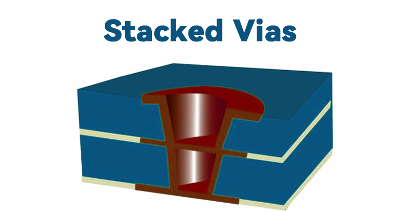
Stacked vias are multiple via stacked vertically on top of each other to connect multiple PCB layers together. Typically, multiple blind or buried via are stacked between different layer to form a stable conductive path through plating and filling, which create a stacked via. This process is complex because it requires precise alignment of the vias during PCB manufacturing to ensure a reliable connection through all relevant layers.
The advantage of stacked via is that they allow multiple layer to be connected in the same plane, making it possible for a single layer to be used as both a signal and a power layer. It reduce PCB complexity and the number of layer, is especially useful when space is limited.
Another advantage of stacked via is that they allow signal to pass more directly through multiple layer without interference from nearby alignment or other circuit component such as capacitor or inductor. In contrast, conventional single layer via can cause crosstalk problem due to nearby alignment, especially in high-frequency circuit. As a result, stacked via offer an advantage in signal integrity for high speed PCB where signal quality needs to be maintained.
Stacked via allow for more compact component packaging because it reduce the number of interconnection required between different layer of a chip stack, thereby reducing manufacturing costs. At the same time, this perforation design create multiple heat transfer path between each layer, allowing heat to dissipate more efficiently. Stacked vias can also provide multiple conductive surfaces, allowing electrostatic discharge (ESD) current to be diverted through multiple paths, reducing the risk of damage from static build up.
6.Staggered Vias
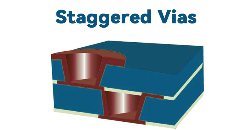
The main feature of staggered through-holes is that multiple through-holes are staggered rather than stacked directly on top of each other. This design frees up more space for wiring and increases flexibility in circuit design.
Benefits of staggered vias:
- Improved space utilisation: Since the holes in staggered via are not perfectly aligned, it effectively free up space on each layer for more wiring or tighter component alignment.
- Simplified Manufacturing: Creating staggered vias is easier, in manufacturing compared to stacked vias because the latter involves an intricate copper filling process due to the need for align holes, across multiple layer of the material. Staggered via do not require such filling, so the manufacturing process is simpler and there is less opportunity for error.
- Reduced cost: Staggered via require less copper filling of the PCB, which save material and reduces manufacturing time. This simplification of the manufacturing process and reduction in time results in lower overall production costs.
Design considerations for staggered vias:
- Controlled wiring length: Because signal path of different length may result in inconsistent delay in signal transmission, which can cause timing problem and signal distortion. On critical signal paths, PCB designer should ensure that each path has a similar electrical length. This will keep the signals synchronised during transmission so that they arrive accurately.
- Crosstalk: Crosstalk is a common problem in staggered via PCB designand is especially likely to occur on densely wired PCB. Crosstalk means that signals on one signal path interfere with signals on neighbouring paths, resulting in lower signal quality and possibly even data loss. In a staggered vias design, engineers can reduce crosstalk by increasing the spacing between alignment. In addition, the design can use grounding layers at critical locations to isolate signal line and further reduce interference problems.
- Impedance control: Impedance is a measure of how well an alignment resists current and directly affects signal integrity. Unstable impedance can lead to signal distortion or reflection phenomena, or even lead to data transmission error. Staggered vias tend to introduce discontinuities in the source destination path, making them unsatisfactory for controlled impedance requirements. Therefore, the impedance of the alignment must be precisely controlled in the design to ensure stable signal transmission.
7. Skip Vias
The skip in skip via refers to the skipping of one or more circuit layers so that two non-adjacent circuit layers are connected. It can be a blind hole, a buried hole or an overlapped hole. When designing PCBs with skip vias, it is important to be aware of the manufacturing constraints and routing plans. the reliability of the skip vias depend on the aspect ratio of the via, so the thickness of the outer layer must be kept within reasonable limits, usually no more than two stacks.
Since Skip Via vias are typically used in the BGA area, the routing paths need to be specifically planned to ensure that the outer layer is thin and meets the aspect ratio requirements underneath the BGA. At the same time, the alignment of the layers that are not connected by the Skip Via needs to be planned in advance in order to avoid the problem of non-transmission of signals.
8.Vias in Pad
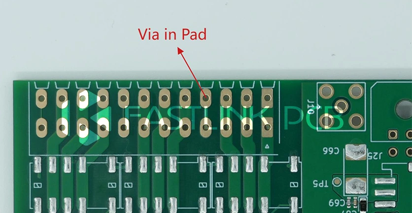
Via-in-Pad is where the vias are placed inside the SMD pads, avoiding the need to route traditional vias to save surface space. They are often found in HDI PCBs and high-frequency PCBs with BGA-packaged ICs.
In addition, the via hole in the pad improve heat dissipation, helping to quickly remove heat from component and layer. It also reduce parasitic inductance by placing the via directly on the pads, eliminating the need for additional connecting segment and reducing overall inductance. In addition, this design allow the bypass capacitor to be placed close to the component, which further reduces inductance. This reduction is very beneficial for high speed signal designs.
However, Via-in-Pad technology also presents some drawback. Firstly, manufacturing costs are high, as creating the vias inside the pads require additional conductive filler material (conductive epoxy or other conductive filler) and processes that do not decrease significantly with volume. Secondly, inaccurate filling may result in surface bumps that can affect the solder quality of small components. In addition, designing and realising such structure is more complex and require a higher level of expertise on the part of the designer. Therefore, these factor need to be carefully weighed before deciding to use Via-in-Pad.
Final Thoughts
These are the basic features and application scenarios of the 8 types of vias in PCB design. Whether they are blind vias, buried vias, or stacked or staggered vias, their unique functions are irreplaceable. How to make full use of the characteristics of these vias in the design, flexible combination to optimise routing and improve space utilisation is the challenge for every designer. We hope that this article will provide you with some practical ideas for your PCB design and help you achieve the desired results in your projects!