- On January 12, 2025
- In blog
How to Reduce PCB Manufacturing Costs? –Molding Beveled Edge Process
Are you also worried about PCB manufacturing cost? As a PCB manufacturer, we are always thinking: how to help you better control cost? Recently, we have made a new breakthrough in the molding pcb beveled edge process, and successfully realized the multiplication of efficiency and significant cost reduction. Let me share the good news with you and see how we did it.
What Is a PCB Beveled Edge?

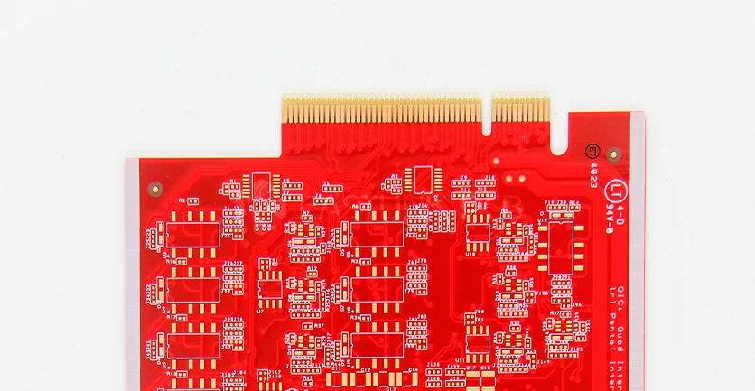
Beveling is one of the PCB molding methods, which is commonly used on gold finger PCBs. It is mainly used to deal with PCB edges, and the board edges are cut into a certain angle by the beveling machine to meet the product assembly or specific functional requirements. According to the application requirements, the form of beveled edges mainly includes the following kinds:
1. Whole edge beveling: the whole edge is processed into beveling usually can be easily done by beveling machine.
2. Partial jump beveled edge: only part of an edge needs beveling treatment, the process complexity is higher, and some beveling machine are difficult to process accurately.
3. Inside beveled edge: beveled edge are located in the inner four sides of the PCB which requires higher precision processing, and is generally difficult to complete by the beveling machine.
Main Difficulties in Molding Bevelled Edges
1. Inefficient Production:
In the process, certain PCB products (e.g., 2pcs spliced 1set design) require complex beveling of four edges, and two of the edges are jump beveled. This design usually requires multiple steps to complete, including: Pre-process ➔ V-CUT ➔ Punching the board ➔ L1-side gong beveling ➔ L2-side gong beveling ➔ Post-processing
In the conventional method, each Set is handled and shipped individually, hence the employees are greatly involved in the handling function while the gong machine itself requires only 30 seconds to complete a cycle. This imbalance resulted in a significant drop in overall productivity.
2. Heavy Burden on Operators:
Beveling is extremely demanding especially with jump bevel or complex design. Operator are required to frequently load and unload every 2 set while maintaining a high level of concentration to avoid missing beveled edge. However the lack of clear identification in the internal design of a set can lead to bad bevel if a slight oversight is made.
How Can We Reduce Your Costs by Optimizing the Beveling Process?
After analyzing the current production process in detail, we found that just increasing the manpower input could not solve the efficiency problem fundamentally. After in-depth discussions with our team, we believe that we must start from the process and design optimization in two directions. Since the design of the Set is customized according to your specific needs, we are not in a position to make too many changes to it, but we can make innovative anti-deactivation design in the panel work side.
Existing Process:
We use a 90-degree gong beveling cutter at the top, and the center of the gong cutter needs to be offset from the edge of the punched board by 0.3mm. Each time we process, the gong machine can only bevel 2 sets, and the operator needs to load and unload the board for each set, which is really a room for efficiency improvement.
What if we change our thinking and finish the beveled edges of the panel before the punching process?
This not only will the task of loading and unloading the beveled edges be much easier, but we can also create specific anti-failure markings on the panel’s working surface to ensure that the right beveled edges are not missed. Even more exciting is the fact that with the help of the distance between sets, our beveling knives can process two edges at once which will be a huge improvement in efficiency!

Is This Program Specifically Feasible? Let’s Take a Look at the Technical Details:
Before the improvement the pitch of the layout was 2.1 mm. If we use an unsharpened beveling knife, the product will be broken on both sides, which will obviously affect the subsequent punching process. If we only modify the layout spacing without adjusting the beveling knife, then the spacing is only 0.3mm, which also affects the quality of the punched board.
After Repeated Verification, We Found the Best Solution:
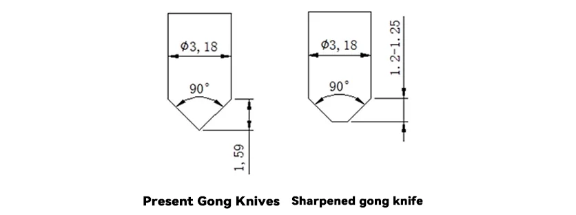
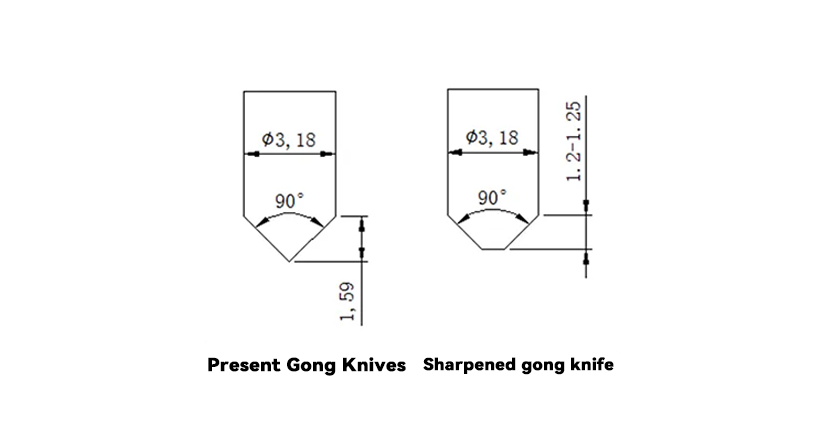
At the same time, we adjusted the spacing between the plates and the length of the beveling knives. After this process, the finished beveled edges on both sides can still maintain a 0.48mm joint, ensuring that the sheet will not be disconnected and the punching operation can be carried out smoothly. Even better, by maintaining a 1.0mm spacing between the long edges of the sets, two sets can be beveled at the same time. Of course, this required adjusting the offset of the beveling gong from 0.3mm to 0.5mm, and we also adopted a new method of checking the first piece of the beveled edge.
Considering That We Moved the Beveling Process Ahead of the Punching Process, This Presented a Challenge:
the dimensional specifications of the bevel could only be measured directly after the punching process was completed. If there is a problem with the beveling process, it can only be detected after the punching process. Especially when adjusting the first piece it is not an ideal process design to have to go through the mold to punch the plate to verify compliance.
Is There a More Convenient Way to Confirm the Dimensions of a Beveled Edge?
Through in-depth simulation and analysis of bevel deviation, we found an interesting pattern: Since the angle of the bevel is 45 degrees, the dimensional changes in the vertical and horizontal directions are exactly the same. Whether it is the offset of the upper and lower depths, or the offset of the left and right alignment, it can be determined by observing whether the hole intersects with the beveled edge or not.
Based on this discovery, we carefully designed 12 npth holes on the working side of the panel, 4 of which are used for individual beveling to confirm the first piece, while the remaining 8 are distributed in the four corners of the panel to monitor the possible rise and fall or shift of the product during the production process. This design brought significant improvements: from the previous need to use measuring tools to obtain data to determine, to a simple visual observation can be completed to check, not only to improve the efficiency of the first piece of debugging, but also to make the inspection more convenient.
Although we have improved the efficiency to a certain extent through the anti-defective design introduced earlier, it is still necessary to observe the board surface one by one in order to check whether there is any missing beveled edge on each panel board. This is time-consuming, and the operator is susceptible to visual fatigue, which can lead to errors in judgment.
For This Reason, We Came Up With a Smarter Solution:
Add a bevel notch to each of the two outermost sides of the panel edge and set this notch as the last part of the bevel program. In this way, checking for missing beveled edges is extremely simple: just place the batch neatly and recognize it by looking at the notches. This not only greatly improves the ease of operation, but also avoids visual fatigue due to the ability to observe a large number of products at once.
How to Do Quality Control?
As a responsible PCB manufacturer, even if we optimize the process, quality control is still the most important thing. As the panel is beveled and then punched, a portion of the punched board will be beveled, which may slightly affect the cutting force of the mold. Therefore, we pay special attention to the burrs on the edge of the punched plate and insist on regular sampling inspections during the production process to prevent any possible process fluctuations from affecting the quality of the product.
How Effective Have We Been in Improving?
1. Labor Cost Reduction by 40%-50%
By adjusting the board beveling process to before punching the board, we have realized an exponential increase in efficiency. Especially for small size SET products, the efficiency improvement is more significant, which means the same labor input can complete more output.
2. Equipment Utilization Rate Increased by More Than 30%
Previously: Front process ➔ V-CUT ➔ Punching ➔ L1-side gong beveling ➔ L2-side gong beveling ➔ Back process
Now: Pre-process ➔ V-CUT ➔ L1-side gong beveling ➔ L2-side gong beveling ➔ Punching ➔ Post-processing
Through process optimization, we have improved the efficiency of equipment use and reduced the idle time of equipment thus reducing the production cost.
3. Cost Benefits From Quality Improvement
The new beveling process significantly improves the product passing rate and reduce rework and material waste.
4. Room for Future Cost Optimization
We found that according to different beveling angles and the specific conditions of punching and gong boards, we can also try to use V-CUT for beveling which may bring even greater cost advantages.
Final Thoughts
The above is about FastlinkPCB’s beveled edge process improvement. We believe that only by helping our customers to reduce costs and improve competitiveness is a true win-win cooperation. In the future, we will continue to be committed to process innovation, to provide you with more cost-effective PCB manufacturing solutions. If you have any idea about our improvement program or cost control, please feel free to communicate with us!