Category Archives: Blog
Comments Off on PCB Manufacturing: FQC Inspection Standardized Process
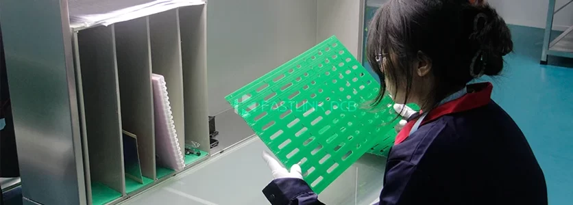
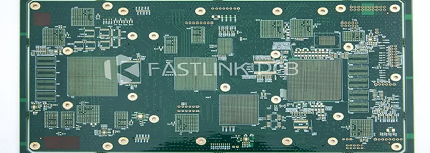
PCB Manufacturing: FQC Inspection Standardized Process
Quality control drives PCB manufacturing. With 15+ years of experience, Fastlink developed strict FQC (Final Quality Control) processes. It covers all steps – from checking basic specs to finding microscopic defects. We aim for zero defects. Our one-stop PCB solutions serve: Industrial electronics Telecom equipment Medical devices Step 1:...
Read More
- On March 28, 2025
- In blog
Comments Off on 3 Points to Know BGA: Features Soldering and X-ray Inspection
3 Points to Know BGA: Features Soldering and X-ray Inspection
Nowadays, electronic products are getting thinner and smaller, but more and more powerful. There is a key role behind this: BGA packaging technology. When a chip needs to be crammed with hundreds of interfaces and compressed to its maximum size, traditional packages are no longer able to do so....
Read More
- On March 14, 2025
- In blog
Comments Off on High Frequency PCB Substrate | Isola, Rogers, Arlon, Taconic,
High Frequency PCB Substrate | Isola, Rogers, Arlon, Taconic,
High-frequency PCB design is often jokingly called “black magic” by engineers, from the material selection stage is full of challenges. Currently on the market, Rogers, Isola, Taconic, Arlon and other big brands provide a variety of unique high-frequency substrates, but the complexity of the data on the parameter table...
Read More
- On January 17, 2025
- In blog
Comments Off on Exploring Common Problems in PCB Engineering Review
Exploring Common Problems in PCB Engineering Review
In the PCB industry, the successful delivery of every order is dependent on a rigorous engineering audit. You may ask: Why is engineering audit so important? This is because a large number of practice has proved that an incomplete or inaccurate order information, often lead to production interruptions, repeated...
Read More
- On January 12, 2025
- In blog
Comments Off on How to Reduce PCB Manufacturing Costs? –Molding Beveled Edge Process
How to Reduce PCB Manufacturing Costs? –Molding Beveled Edge Process
Are you also worried about PCB manufacturing cost? As a PCB manufacturer, we are always thinking: how to help you better control cost? Recently, we have made a new breakthrough in the molding pcb beveled edge process, and successfully realized the multiplication of efficiency and significant cost reduction. Let...
Read More
- On December 3, 2024
- In blog
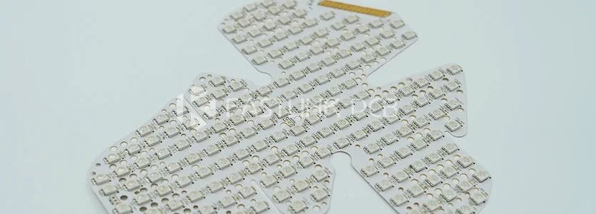
Comments Off on What Do You Need to Know About LED PCBs
What Do You Need to Know About LED PCBs
Light-emitting diodes (LEDs), an increasingly popular lighting technology, are being used in a wide range of industries, from gaming device and lighting system to home décor and industrial human-machine interfaces. As a solid-state lighting device, LED convert electricity into light through semiconductors, reducing energy consumption by up to 80%...
Read More
- On November 19, 2024
- In blog
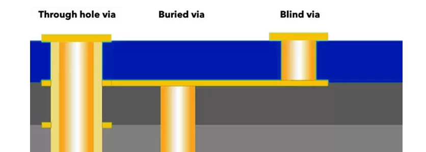
Comments Off on 8 Types of Vias on a PCB: Design Details You Need to Know
8 Types of Vias on a PCB: Design Details You Need to Know
Holes in PCB help us with circuit connection, signal transmission and space optimisation. Different types of holes provide designers with a variety of way to do this, but they also differ in their design characteristics. In the next section, we will introduce the eight major PCB hole type to...
Read More

- On November 8, 2024
- In blog
Comments Off on 9 Key Factors Affecting PCB Thickness
9 Key Factors Affecting PCB Thickness
Thickness is a key parameter in the design and manufacture of PCB, affecting the performance and suitability of the PCB. So, how to determine the appropriate PCB thickness? In fact, the thickness of the PCB is not set in stone, it is affected by a variety of factor. Different...
Read More
- On September 5, 2024
- In blog
Comments Off on How to Choose Between Aluminum PCBs and Copper PCBs?
How to Choose Between Aluminum PCBs and Copper PCBs?
In the era of ever-increasing miniaturization and escalating power density of electronic devices, the thermal dissipation capabilities of PCB substrates have emerged as a pivotal factor influencing product reliability. Renowned for lightweight nature and ease of processing, aluminum substrates stand out; while copper substrates boast remarkable electrical conductivity and...
Read More
- On August 26, 2024
- In blog
Comments Off on Comparison of High-Frequency PCB and High-Speed PCB
Comparison of High-Frequency PCB and High-Speed PCB
High speed and high frequency PCB play a role in powering 5G and IoT technologies. While some people consider them interchangeable, there are subtle distinctions in their intended purpose. This article delves into the technical aspects that differentiate them offering a comprehensive understanding of their design and manufacturing processes....
Read More