- On August 26, 2024
- In blog
Comparison of High-Frequency PCB and High-Speed PCB
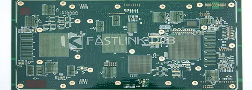
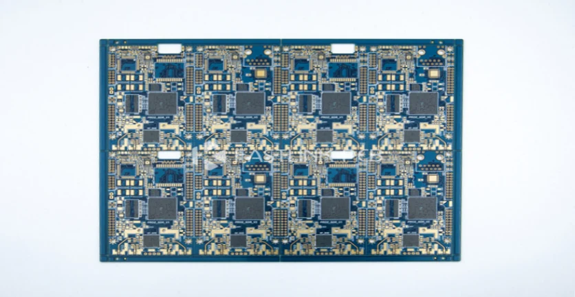
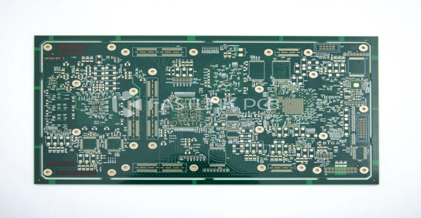
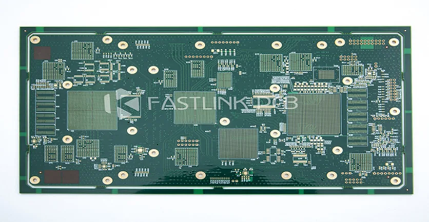
High speed and high frequency PCB play a role in powering 5G and IoT technologies. While some people consider them interchangeable, there are subtle distinctions in their intended purpose. This article delves into the technical aspects that differentiate them offering a comprehensive understanding of their design and manufacturing processes.
What Are High-Frequency and High-Speed PCB?
Before you know their definitions, I have to explain the units that describe frequency and data transfer rate. MHz (Megahertz) is a unit of frequency that measures the number of cycles per second in a signal or wave, with 1 MHz equal to 1 million cycles per second. Gbps, abbreviated from Gigabits per second, quantifies the amount of data transferred per second, 1 Gbps equal to 1 billion bits per second.
High frequency PCBs are usually known as circuit boards created for transmitting signals at high frequencies often surpassing 500MHz. Conversely, high speed PCBs are circuit boards utilized for propagating high speed digital signals. The transmission speeds of these signals typically reach 1 Gbps or more.
Applications of High-Frequency and High-Speed PCB
While high frequency PCBs are mainly utilized in scenarios that necessitate dealing with high frequency signals like in wireless communications, radar systems and testing and measuring devices. High speed PCBs are predominantly found in digital electronics, telecommunications and consumer electronics sectors where rapid data processing and transmission are essential.
The table below outlines the distinctions in their respective application areas. If you need guidance on selecting the right type of PCBs for your specific application feel free to reach out to our engineers.
| Application Area | High-Frequency PCBs | High-Speed PCBs |
| Radar and Satellite Communications | Radar systems Satellite communications Aerospace and defense applications | – Not commonly used |
| Wireless Infrastructure | Base stations Cell towers Wireless network equipment | – Not commonly used |
| Test and Measurement Equipment | Spectrum analyzers Network analyzers Oscilloscopes | – Not commonly used |
| Industrial and Scientific Applications | Medical imaging equipment Industrial microwave ovens Scientific instrumentation | – Not commonly used |
| Digital Electronics | – Not commonly used | Computers Servers Networking equipment |
| Telecommunications | – Not commonly used | Routers Switches Fiber-optic transceivers |
| Automotive Electronics | – Not commonly used | Advanced driver assistance systems (ADAS) Infotainment systems |
| Consumer Electronics | – Not commonly used | Smartphones Tablets Gaming consoles |
Signal Type of High-Frequency and High-Speed PCB
The signal types in high-frequency PCBs are primarily analog, RF, and microwave signals, such as:
- RF signals for wireless communication, radar, and satellite applications.
- Microwave signals for satellite, military, and defense applications.
- Analog signals for high-frequency data links, instrumentation, and control systems.
The signal types in high-speed PCBs are primarily digital signals, such as:
- High-speed digital data signals for computer, networking, and communications applications.
- Clock signals for synchronizing digital circuits.
- Differential signaling for high-speed digital interfaces (e.g., PCIe, SATA, DisplayPort).
Materials of High-Frequency and High-Speed PCB
While the material requirements for high-speed PCBs and high-frequency PCBs indeed share numerous similarities due to their involvement in the transmission and processing of high-frequency signals, their specific design emphases diverge, potentially leading to distinct material selection criteria.
Similar Materials
The materials utilized in both high-speed and high-frequency PCBs necessitate a low dielectric constant (Dk) for minimal signal delay and stability, a low dissipation factor (Df) to reduce signal loss, excellent thermal stability for maintaining consistent performance under varying temperature conditions, and low dielectric loss for efficient energy transmission.
Different Materials
High-frequency PCBs perform at extremely high frequencies (e.g., GHz and above), hence material selection heavily favors those that excel in ultra-high frequency environments. At Fastlink, we often use PTFE (Polytetrafluoroethylene) and ceramic-filled materials to fabricate high-frequency PCB. These materials are known for their superior electrical properties, which are crucial for maintaining signal integrity and minimizing losses. Below are some of the commonly used brand for high-frequency PCBs:
| Material Brand | Material Series |
| Rogers | RO4000 Series RT/duroid Series TMM Series |
| Taconic | TLY Series RF-35 |
| Isola | IS620 Astra MT77 |
| Arion | AD Series CLTE |
| Panasonic | Megtron 6 R-F775 |
| PTFE (Teflon) | General PTFE |
| Nelko | N4000-13 N7000 |
High-speed PCBs primarily focus on data transmission speed (e.g., Gbps), while involving high-frequency signals, do not necessarily operate at the extremely high frequencies encountered in high-frequency PCBs. Their frequency range, however, can be broader. Consequently, Fastlink suggests that opt for modified FR4 materials that offer a balance between cost and performance.
Design Challenges of High-Frequency and High-Speed PCB
Designing high frequency PCB and high speed PCB confront numerous shared obstacles, due to their common involvement in transmitting high frequency signals and handling high speed data.
Similar Design Challenges
Signal Integrity (SI)
High-frequency and high-speed signals are susceptible to degradation, signal reflections, crosstalk, and noise, we employ careful routing of trace, precise impedance control, and advanced shielding techniques to ensure signal integrity.
Impedance Control
Accurate impedance control is critical for high frequency and high speed PCBs to maintain signal integrity, support high-speed transmission, enable effective filtering and shielding. Fastlink maintains the correct impedance through a combination of precise fabrication techniques, such as tight control over trace width and spacing, PCB stack-up, and material selection, etc.
Electromagnetic Interference (EMI)
As the high-frequency signals can generate significant electromagnetic radiation that can degrade signal integrity through crosstalk and other coupling effects, Fastlink adopts strategies of mitigating EMI including carefully managing the trace layout and routing, implementing a solid ground plane, strategically placing decoupling capacitors, utilizing shielding and filtering components, and maintaining consistent impedance and layer stackup.
Thermal Management
Due to the increased power dissipation from high-speed circuits and components, we’re seeing thermal-related failures like part wear, solder cracks, delamination, warping, broken conductive paths, dielectric breakdowns, and materials and connections aging faster.
To mitigate these issues, Fastlink implements comprehensive thermal management strategies, including effective heat dissipation, like heatsinks and thermal vias, using thermal modeling and simulation to optimize the design, selecting materials with high thermal conductivity, thoughtfully routing traces and layers to facilitate heat transfer.
Different Design Challenges
Layer Stack-up Designs
High-speed PCB frequently uses multilayer constructions, including double, four and six layer, etc., to ensure separation between signal layers and reference planes. However high frequency PCB requires an increased layer count of eight, ten or more to provide sufficient signal layers, reference planes, and shielding layers. Our factory has decades of expertise in producing the latest high-speed and high-frequency PCB. With state-of-the-art equipment and skilled workers, we can manufacture high-frequency PCBs from 8 to 48 layers at frequencies up to 100 GHz and high-speed PCBs with minimum trace widths and spaces down to 2.5 mil.
Routing
Generally speaking, the widths and spacings of traces in high speed PCB are narrower compared to those in high frequency PCB, this is because tight layout is crucial in high speed PCB design to facilitate high-speed data transmission and reduce crosstalk. Conversely in high frequency PCB, the sizes of the traces and spacings are usually determined by the impedance control, involving wider traces and spacings to preserve signal integrity.
Manufacturing Complexity of High-Frequency and High-Speed PCB
High frequency PCBs are generally more intricate and expensive to fabricate compared to high speed PCB, this can be attributed to the following key factors:
Material Selection and Processing
High frequency PCB needs special materials, such as Rogers RO4003C, RO4350B with low loss and low dielectric constant, which can be challenging to handle, however high speed PCBs can utilize readily accessible materials, like FR4, which are generally easier to manage.
Layer Stackup
High-frequency PCBs often need a greater number of layers, such as 8-layer, 10-layer, or even more, this complex layer stackup poses higher manufacturing requirements. High-speed PCBs typically have a simpler layer structure.
Routing
High frequency PCB uses more precise microstrip and stripline routing due to necessity in handling high-frequency microwave signals, which are inherently more susceptible to variations in trace widths and spacings. Even minute deviations can lead to significant signal distortions, reflections, and impedance mismatches. In contrast, high speed PCB typically deals with digital high-speed signals, exhibits a relatively lesser sensitivity to changes in trace widths and spacings compared to high-frequency signals.
How to choose from microstrip and stripline?
In the realm of high frequency and high speed PCB design, microstrip lines and striplines are two prevalent transmission line structures. At Fastlink, microstrip is often used for high-frequency PCBs. Because high-frequency PCBs need to handle microwave signals, and the simple structure of microstrip makes it easier to design and manufacture.
Stripline is usually used for high-speed PCBs. Because high-speed PCBs need to transmit wideband digital signals across multiple layers, and the shielding performance of stripline is better, however this is not an absolute rule, and the specific design and manufacturing capabilities should be considered.
Metallization Processes
Manufacturing high frequency PCBs requires top notch metallization techniques such as precise laser drilling, plating and polishing to reduce signal loss. The metallization procedures for high speed PCB are less strict.
Testing
At Fastlink, testing high frequency PCBs commonly involves network analysis, spectrum analysis, and a focus on signal behavior at high frequencies. High speed PCBs testing can be relatively simpler, like time-domain reflectometry (TDR), eye pattern analysis, and timing analysis, focusing on signal timing and transmission speed.
Cost of High-Frequency and High-Speed PCB
The cost of high frequency PCB elevates because of higher material bills, more complicated manufacturing, and the need for thorough testing. This makes it pricier than high speed PCB that use more standard, cost saving methods.
| Cost Factor | High-Frequency PCBs | High-Speed PCBs |
| Materials | PTFE, ceramic | FR-4 |
| Layer Stackup | 8-layer, 10-layer, or more | 4-layer, 6-layer |
| Manufacturing Processes | tighter tolerances, specialized equipment | relaxed tolerances, standard equipment |
| Testing | network analyzers, spectrum analyzers | time-domain reflectometry, eye-pattern testing |
| Overall Cost | Higher | Lower |
You may complain about the high materials cost of high frequency PCBs, Fastlink uses a mixed stackup to reduce the costs of high-frequency PCBs – using FR4 for some non-critical signal layers and high-frequency materials in the critical signal paths.
But it requires careful consideration of the tradeoffs. Different materials have different dielectric loss, dielectric constant and impedance, which lead to signal integrity issues such as reflection, distortions and interference. No worries, Fastlink performs thorough simulations and testing to find the optimal material blend and configuration.
Why Choose Fastlink?
Over the years we have gained expertise in producing high speed and HF PCB. We’ve helped over a thousand clients from various sectors such as wireless infrastructure, digital electronics, telecommunications, radar, satellite and beyond. Check our capabilities as follows:
| Feature | Capabilities |
| Layer Count | Up to 48 Layers |
| Line Width and Spacing | Precision to 2.5/2.5 mil |
| Maximum Copper | 3oz |
| Prototype Turnaround Time | As Fast as 5 Days |
| Production Lead Time | As Fast as 3 Days |
| Materials | Rogers, Taconic, Arlon |
| Surface Finish | plating hard gold, ENIG, Immersion Tin, Immersion silver, OSP, ENIG+OSP |
| Frequency Range | 1 GHz to 128 GHz |
| Signal Rate | 128Gbs |
| Certifications | UL, RoHS, ISO 9001, ISO 13485, IATF 16949, AS9100, MIL-PRF-31032, MIL-PRF-55110 |
| Test | eye diagrams, TDR, network analysis, spectrum analysis |
Military Standards
Our high-frequency and high speed PCBs are built tough to handle extreme environments and give you rock-solid reliability. With strict testing and military-grade standards – MIL-PRF-31032, MIL-PRF-55110, they’re perfect for mission-critical applications.
Responsive Customer Support
There are intricate challenges of manufacturing high-frequency PCBs. That’s why we offer 24/7 technical support, from design consultations to post-sale assistance and response within 1 hour of your inquiry.
Experienced Engineers
Fastlink has more than 100 experienced engineers, who are committed to creating top notch PCB for the most challenging uses, focusing on meeting the increasing demands of 5G and IoT.