- On April 16, 2025
- In blog
ENIG vs Hard Gold: Which Is Better for Your PCB?
When choosing a surface treatment, the gold plating process is usually a good choice. Because of the stability of gold, it can effectively resist corrosion and oxidation and provide long-term reliable protection for PCBs. In practice, engineers are usually faced with two choices: ENIG and hard gold. Although both use a gold layer as protection, they differ significantly in cost, durability and applicable scenarios.
In this article, we will analyze the difference between ENIG and hard gold in detail, analyze their respective advantages and disadvantages, and help you make the best choice according to your project needs.
Surface Finish Manufacturing Processes
Although ENIG and hard gold are both gold-containing surface treatments, the differences in their manufacturing principles fundamentally determine their characteristics and applications. In order to understand the difference between the two, we must start with their production processes.
Electroless Nickel Immersion Gold Process
ENIG is a non-electrochemical deposition process that forms a uniform surface protection layer through an autocatalytic reaction.
1.Chemical nickel plating: PCB is immersed in chemical plating solution containing hypophosphates, nickel ions undergo redox reaction on the copper surface to deposit an amorphous nickel-phosphorus alloy layer. This process does not require power, nickel layer can be uniformly covered with complex graphics.
2.Replacement gold immersion: In the nickel layer surface immersed in an acidic solution containing gold ions, through the replacement reaction to form a thin layer of gold (thickness of 0.03-0.1 microns). This gold layer is very thin but pure gold, can isolate oxygen, prevent nickel oxidation and improve solderability.
Hard Gold Plating Process
Different from the working principle of ENIG, hard gold is a surface protection layer realized by electrolysis process.
1.Electroplated nickel layer: The PCB is immersed in an electrolyte and energized, and a layer of nickel is deposited on the copper surface by electrochemical reaction. The nickel layer acts as a barrier layer to prevent diffusion.
2.Electroplated gold layer: continue to energize the nickel layer to make it plated with a hard gold layer (thickness of 0.5-3 microns). The addition of gold element makes the hardness of the gold layer increase significantly and enhances the resistance to mechanical abrasion.
Hard Gold vs. ENIG: Comparison of Features
Through the previous analysis of the manufacturing principles of ENIG and hard gold, it can be seen that the differences in the coating structure, metal composition and deposition methods of the two directly lead to the differences in electrical conductivity, abrasion resistance, solderability and other key properties. Next, we will develop a more detailed comparison from five aspects.
1.Wear Resistance
With its thicker gold layer and the addition of nickel/cobalt alloy, hard gold exhibits excellent abrasion resistance and mechanical strength, making it particularly suitable for high wear applications such as connectors and keyboard contacts. However, it is less flexible and not suitable for scenarios that require bending.
ENIG meets the durability needs of conventional PCBs, but is not suitable for high-wear environments. Its thin gold layer can effectively prevent oxidation and corrosion, but it is more likely to produce scratches due to mechanical friction.
2. Solderability
Hard gold is usually not suitable for direct soldering due to the presence of nickel or cobalt alloys. When soldering is required, additional surface treatment is necessary.
ENIG has excellent solderability and is the first choice for fine pitch components and high density PCB designs. Its flat and smooth surface ensures consistent soldering and is particularly suitable for precision components such as BGAs and CSPs. In addition, ENIG’s self-leveling characteristics make it ideal for automated PCB assembly.
3. Antioxidant and Corrosion Resistance
The thicker gold layer of hard gold provides excellent oxidation and corrosion resistance, which is particularly suitable for aerospace, military and industrial equipment and other harsh environments.
Although the nickel layer of ENIG can effectively block copper diffusion and oxidation, its corrosion resistance is still not as good as that of hard gold. In addition, ENIG may have “black pad” defects (solderability problems due to nickel-gold interfacial contamination), which need to be strictly controlled in the manufacturing process.
4. Process Complexity
The hard gold process is more complex because the plating current and thickness need to be precisely controlled to ensure coating uniformity.
The ENIG process is simpler and easier to automate, which significantly reduces cycle time and costs, and ensures consistent thickness across the board.
5. Cost Comparison
Hard gold is more expensive due to the thicker layer and complexity of the process, but its wear resistance significantly extends product life in high wear applications, thus offsetting the initial cost.
ENIG is more cost-effective and ideal for most standard PCBs, providing a good balance between performance and cost.
Final Thoughts
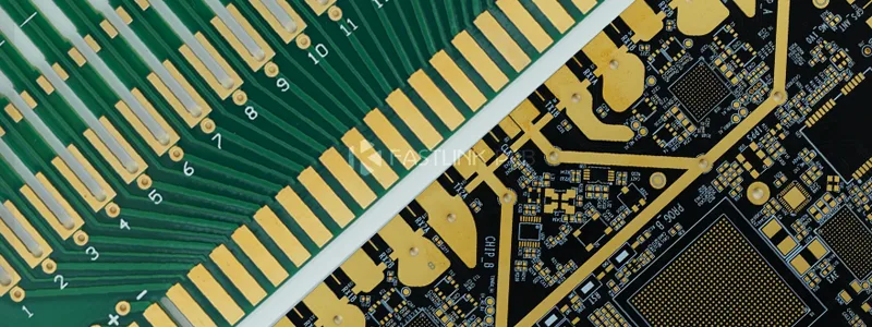
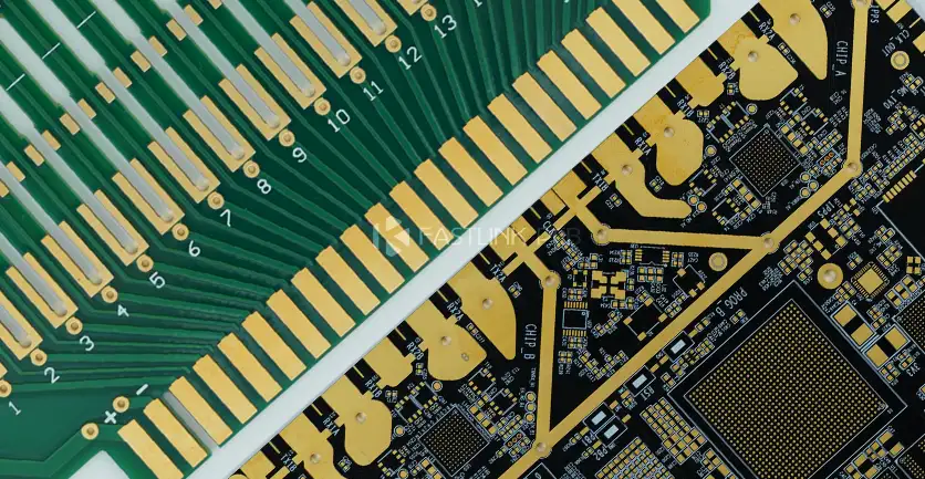
To summarize, hard gold is usually used only in contact areas that require frequent insertion and removal, such as gold fingers, due to its excellent wear resistance properties. However, due to its poor solderability, it is not suitable for soldering areas of PCBs. In contrast, ENIG, as the most commonly used surface treatment process, can be widely applied to the entire PCB surface due to its excellent corrosion resistance and solderability.
If you still have any questions about PCB surface treatment processes, our professional team is ready to provide you with consulting services. Fastlink as a PCB manufacturing expert with 15 years of industry experience, can provide all the mainstream surface treatment processes, including HASL, ENIG, OSP, immersion silver, ENEPIG, hard gold plating and immersion tin, to ensure that your PCB products are perfectly adapted to a variety of application scenarios. We ensure that your PCB products are perfectly adapted to various application scenarios.