- On June 13, 2024
- In blog
What Is Exposure in PCB Production?
Exposure in PCB Production refers to the stage where a photoresist, applied on the PCB substrate is exposed to a light source usually ultraviolet (UV) light, this light exposure triggers a chemical reaction, which can change the properties of the photoresist.
What Is Photoresist in PCB Production?
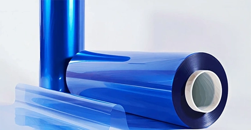
Photoresist, or dry film is a light-sensitive material coated on PCB substrate in exposure process during printed circuit board manufacturing to create precise circuit patterns on the board. It undergoes chemical changes when exposed to light. These changes allow selective removal of areas during development and etching processes.
Chemical Changes When Photoresist Exposed to Light
In the realm of PCB engineering, photoresists are differentiated into two primary types: positive and negative. Each type performs unique chemical reactions when exposed to light. The solubility of the exposed or unexposed regions in the developer solution is contingent upon the specific type of photoresist utilized.
Chemical Principle of Positive Photoresist
Positive photoresist typically contains a Photo Acid Generator. Under Ultraviolet light exposure, the PAG decomposes to produce acidic substances. These acidic substances further induce a breakage reaction in the main chain of the photoresist, making the exposed areas soluble in the developer solution.
Chemical Principle of Negative Photoresist
Negative photoresist usually includes a photoinitiator. When exposed to ultraviolet light, the photoinitiator produces free radicals. These free radicals facilitate cross linking reactions among the photoresist molecules, which renders the exposed sections resistant to dissolution in the developer solution.
General Steps of the Exposure in PCB Production
The exposure process in PCB manufacturing, particularly when using methods such as projection printing generally involves the following steps:
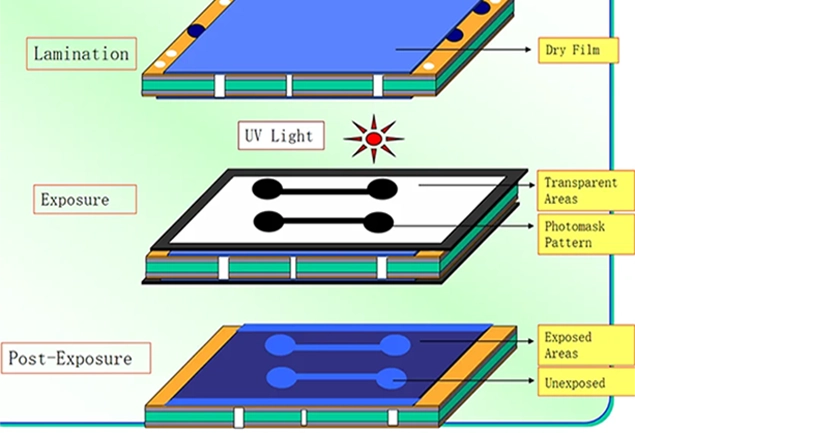
Preparation: The PCB substrate is meticulously coated with a layer of photoresist. This light-reactive compound, available in both liquid and dry film versions, is sensitive to ultraviolet light. Upon exposure to UV light, this photoresist layer will experience a series of chemical transformations.
Placement: In the context of projection printing, the photomask is strategically positioned within the exposure machine. Serving as a stencil, the photomask selectively permits or restricts light transmission to the photoresist layer, thereby ensuring precision in the circuit design process.
Exposure: The photoresist is exposed to a light source, which could be a UV laser or LED, contingent on the specifications of the exposure equipment. This light source projects the photomask’s image onto the photoresist layer. The photomask’s opaque regions obstruct light exposure, whereas its transparent sections permit it. Given the light-sensitive nature of the photoresist, only the regions exposed to light undergo chemical alterations, thereby establishing the circuit pattern.
Main Exposure Techniques
Different exposure techniques has its own advantages and applications, depending on the requirements for precision, efficiency, and scalability.
Contact Printing
Contact Printing is a fundamental lithographic process used in PCB and semiconductor manufacturing where a photomask is placed in direct contact with a photoresist-coated substrate during exposure to a light source, usually UV light. This direct contact ensures that the mask’s pattern is sharply and accurately transferred onto the photoresist, allowing for precise replication of fine details.
The method is straightforward and cost-effective, making it ideal for producing simple and less complex circuit patterns.
However, the close contact can lead to wear and potential damage to both the mask and the substrate, and it is less suitable for high-resolution or densely packed designs compared to more advanced techniques like projection printing or direct imaging.
Proximity Printing
Proximity Printing is a lithographic technique used in PCB manufacturing where a photomask is placed in close, but not direct, contact with a photoresist-coated substrate during the exposure process. Typically, the mask is positioned a small distance (micrometers to tens of micrometers) above the substrate, allowing light to pass through the mask’s transparent areas and project the desired pattern onto the photoresist.
This gap helps reduce wear on the mask and substrate while maintaining higher resolution than contact printing. Proximity printing is useful for applications where slight non-contact can minimize defects and extend the lifespan of the photomask, but it is generally less precise than projection or direct imaging methods, making it more suited for less critical or less densely packed circuit designs.
Projection Printing
Unlike traditional contact or proximity printing methods, where the photomask is placed directly on or near the substrate, projection printing uses a system of lenses to project the mask image onto the photoresist from a distance.
This technique allows for high-resolution patterning with fine detail and less physical wear on the mask and substrate.
Disadvantages: More complex and expensive equipment, potential alignment issues with large substrates.
Direct Imaging (DI)
Direct Imaging is an advanced technique used in PCB manufacturing to transfer circuit patterns directly onto a photoresist-coated substrate without the need for traditional photomasks. Utilizing precision-controlled laser or UV light sources, DI systems digitally project the desired pattern directly onto the board, precisely exposing the photoresist in the intended areas.
This method offers significant advantages over conventional methods, including greater flexibility in design modifications, higher resolution, and the ability to produce fine features and intricate details. DI also reduces production time and costs associated with mask creation and handling, making it ideal for complex and high-density PCB designs, quick-turn prototyping, and small-batch production.
Factors Affecting the Quality of Exposure
Alignment Accuracy
A photomask (or photo tool), which contains the desired circuit pattern, is precisely aligned over the photoresist-coated PCB. The photomask acts as a stencil, selectively blocking or allowing light to pass through to the photoresist layer. Misalignment can result in distorted or incomplete circuit patterns.
Light Source Quality
The intensity and uniformity of the UV light source affect the exposure. Inconsistent light can lead to uneven exposure, causing variations in the photoresist development. It is required that the main absorption peak of the photoresist spectrum overlaps or mostly overlaps with the main emission peak of the light source. Among various light sources, dysprosium lamps, high-pressure mercury lamps and iodine gallium lamps are suitable, while xenon lamps are not suitable.
Photoresist Quality
The quality and state of the photoresist can affect how it responds to UV exposure. Photoresists that are old or stored improperly may not react as expected.
Exposure Time
Getting the exposure time right is crucial. Much exposure can make the photoresist too hard leading to residues, while too little exposure can leave it underdeveloped, resulting in unclear lines, dull color, and even debonding.
Environmental Conditions
Factors, like temperature, humidity and cleanliness in the exposure environment can impact the process. Dust or contaminants can block UV light, affecting the photoresist’s reaction.
Photomask Quality
The quality and condition of the photomask are factors to consider. Any defects, scratches, or impurities on the photomask can lead to flawed circuit patterns.
Substrate Quality
The condition of the PCB substrate itself, including its surface smoothness and cleanliness, plays a role in ensuring uniform exposure.
Equipment Calibration
Regularly maintaining the exposure machine ensures that it operates according to the specifications, providing consistent results.
The Role of Exposure in PCB Manufacturing
Exposure in PCB manufacturing is a crucial step that plays a vital role in defining the precise patterns and structures on a printed circuit board. During this process, a photoresist-coated substrate is exposed to a controlled light source, typically ultraviolet light. This exposure transfers the desired circuit design onto the photoresist layer, which acts as a temporary protective mask.
Pattern Transfer
Function: Exposure accurately transfers the circuit patterns from a photomask or digital file onto the photoresist layer.
Significance: This step is fundamental in defining the precise geometric shapes of the conductive paths and features of the PCB, ensuring that the intended design is faithfully reproduced.
Selective Development
Function: After exposure, the photoresist undergoes a development process where the exposed or unexposed areas (depending on whether a positive or negative photoresist is used) are removed.
Significance: This selective development reveals the underlying copper areas that will be etched away or retained, forming the actual conductive traces and pads on the PCB.
High Resolution and Fine Detail
Function: Advanced exposure techniques, such as direct imaging, can achieve very high resolutions, allowing for the creation of intricate and densely packed circuit designs.
Significance: This capability is crucial for modern PCBs, especially in applications requiring high precision, such as high-frequency or high-speed electronics, where small feature sizes and tight tolerances are essential.
Layer Alignment
Function: In multi-layer PCB manufacturing, exposure helps align different layers accurately by using alignment marks or fiducials on the substrate.
Significance: Proper alignment ensures that vias and interlayer connections align perfectly, which is critical for the electrical performance and structural integrity of multi-layer boards.
Process Efficiency
Function: Exposure processes, particularly with digital direct imaging, allow for rapid and flexible patterning without the need for physical masks.
Significance: This increases production efficiency and reduces the time and cost associated with mask production and handling, enabling quicker turnaround times and the ability to easily accommodate design changes.
Consequences of Poor Quality Exposure
If transferring circuit patterns onto a photoresist-coated substrate using light, is not accurately controlled, it can result in incomplete or excessive exposure. These issues may cause improper development of the photoresist, leading to defects such as undercutting or over-etching. Such defects can alter the intended circuit pathways, resulting in signal loss, short circuits, or open circuits.
Inconsistent exposure can affect the alignment of multi-layer PCBs, causing misalignment of layers and vias, which are essential for the electrical connectivity between layers.
Poor exposure quality can also degrade the precision and resolution of fine features, impacting the functionality of high-density and high-speed circuits.
Consequently, ensuring precise and consistent exposure is crucial to maintaining the integrity, performance, and longevity of the PCB.
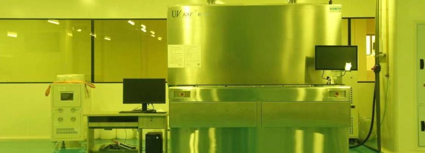
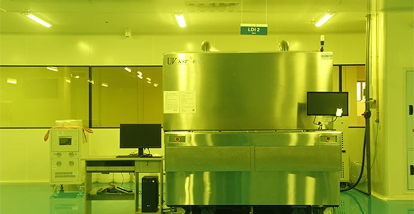
Fastlink’s Cutting-Edge LDI Exposure Solutions
Fastlink’s LDI technology uses high-resolution lasers to directly write circuit patterns onto the PCB photoresist. This eliminates the need for traditional photomasks, ensuring the highest levels of accuracy in the complex designs. This mask-free approach accelerates production cycles, reduces costs, and allows for immediate pattern changes, making it ideal for rapid prototyping and high-density interconnects (HDI).
Contact us today to experience the next generation of PCB production with Fastlink.