- On April 2, 2025
- In blog
PCB Manufacturing: FQC Inspection Standardized Process
Quality control drives PCB manufacturing. With 15+ years of experience, Fastlink developed strict FQC (Final Quality Control) processes. It covers all steps – from checking basic specs to finding microscopic defects.
We aim for zero defects. Our one-stop PCB solutions serve:
- Industrial electronics
- Telecom equipment
- Medical devices
Step 1: Receive Boards
① Information Check
After receiving PCB units, we verify:
- Order details (model, quantity, revision)
- Surface finish (e.g., ENIG, HASL)
- Process card (matches specifications)
② Stacking Rules
We adjust stacking by thickness:
- ≤1.0mm: 50 boards/stack
- >1.0mm: 20 boards/stack
Staggered stacking prevents scratches and warping from pressure.
Step 2: Pick Up Boards
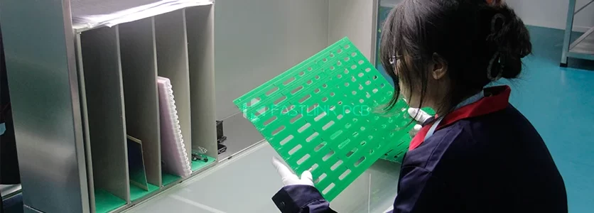
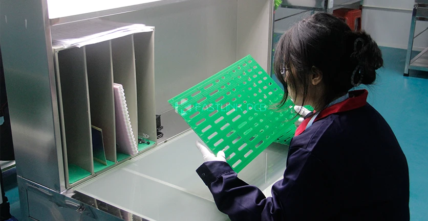
① Dust-Free Handling
Inspectors must:
Wear anti-static gloves/finger cots
Hold boards with both hands
Prevents fingerprints & electrostatic damage.
② Inspection Table Prep
Daily cleaning & sterilization required
Zero particulate debris allowed
③ Board Placement
Align PCBs uniformly (same surface/direction)
Use custom fixtures for:
✓ Fast hole/slot positioning
✓ 30%+ efficiency gain
Step 3: Inspection Information
At Fastlink, every PCB undergoes a 360° quality verification protocol. Our 5-stage inspection cascade combines:
1.Basic Information Verification

①Model/Quantity/Revision Check
✓ Match process card vs. physical board
✓ Confirm:
- Model number
- Total quantity
- Revision level
②Solder Mask & Silkscreen Color Check
✓ Verify colors meet customer specs:
- Solder mask (e.g., green, black)
- Silkscreen (text/logo)
✓ No color bleeding/mismatch
③Test Line & ET Stamp Inspection
- Test line position & continuity
- ET stamp legibility (clear marking)
2.Process Parameter Verification
① Solder Mask & Via Plugging
✓ Solder mask window opening – Verify precision (no misalignment)
✓ Via plugging – Check for:
- Full filling (no voids)
- No glue leakage/overflow
② Silkscreen (Character) Inspection
✓ Print quality:
- Sharp, unblurred text/logos
- No positional offset (per design file)
✓ Critical areas: High-density zones (e.g., near ICs)
③ Surface Finish Compliance
✓ Type & thickness:
- ENIG (Immersion Gold) / HASL (Tin Spray) / OSP
- Measure thickness (e.g., Au ≥0.05μm)
✓ Defect screening:
- No oxidation (gold surfaces)
- No plating leakage
3.Structural & Functional Tests
① Outline (Gong Plate) & V-Cut
✓ Edge flatness: ≤0.1mm warpage
✓ V-Cut depth: ±5% of board thickness
✓ Defects: No burrs/chips
② Countersunk Holes
✓ Depth tolerance: ±0.03mm (laser-measured)
✓ Verify against customer drawings
③ Electrical Tests
✓ Continuity test: 100% circuit functionality
✓ Impedance test: Match spec (e.g., ±10% for 50Ω lines)
4.BGA Special Inspection
① Pad Alignment
✓ X-ray check:
- Offset tolerance: ≤25% of pad diameter
- Prevent soldering defects
② Pad Dimensions
✓ Diameter/spacing: Match design specs (e.g., ±0.05mm)
5.Surface Defect Screening
① Silkscreen Defects
✓ No breaks/sticking (200x magnification)
✓ High-density areas: Extra scrutiny
② Oxidation & Contamination
✓ ENIG boards:
- Uniform gold color (no black pads)
✓ HASL boards:
- Smooth tin surface
- No tin beads
Step 4: Automated Verification

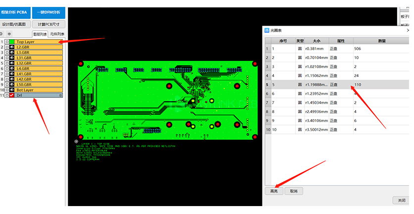
① Intelligent Aperture Inspection
✓ Software workflow:
- Import customer Gerber/ODB++ into CAM software (Genesis/Huaqiu DFM)
- Auto-generate aperture report (focus on ≥0.5mm features)
✓ Measurement protocol:
- Verify 100% of critical apertures
- Tolerance: ±0.025mm for plated holes
- Flag any missing/drilling deviations
② Profile Data Verification
✓ Layer comparison:
- Match production GKO/BOX layers to physical board
- Critical parameters:
- V-CUT depth: ±0.05mm
Step 5: Panel Handling & Stacking
① Handling Protocol
✓ ESD control:
- Mandatory anti-static gloves (surface resistance 10⁶-10⁹Ω)
- Two-hand corner grip
✓ Damage prevention:
- No direct contact with copper traces
- 30° angle placement
② Stacking Configuration
✓ Thickness-based rules:
| Thickness | Stack Height |
| ≤1.0mm | 50 panels |
| >1.0mm | 20 panels  |
③ Orientation Standardization
✓ Alignment requirements:
- All fiducials facing same direction
- ET stamps within 5° deviation
✓ Automated verification:
- Barcode scanner confirms panel orientation
- Vision system checks marking consistency
④ Dimensional Inspection
✓ Automated measurement:
- Laser micrometer verifies stack uniformity
- Tolerance: ±0.2mm overall thickness
✓ Defect screening:
- 10x magnification for edge defects
- No visible tooling marks (Ra ≤3.2μm)
Step 6: V-CUT Quality Assurance
① Optical Transmission Inspection
✓ Equipment:
- 5000K LED backlight (≥2000 lux intensity)
- 10x digital microscope with coaxial illumination
✓ Acceptance Criteria:
- Straightness tolerance: ≤0.1mm/100mm length
- Zero copper residual at cut lines
- No micro-jagged edges (Ra ≤6.3μm)
② 360° Micro-Crack Detection
✓ AOI Configuration:
- 5MP telecentric lens (10μm resolution)
- Four-axis rotary fixture (±0.5° positioning accuracy)
✓ Defect Parameters:
- Crack detection threshold: ≥25μm length
- Scanning speed: ≤15 sec/panel
③ Dimensional Verification
✓ Depth Measurement:
- Laser confocal sensor (0.001mm resolution)
- Sampling rate: 5 points per V-CUT
- Tolerance: ±0.05mm (Class 3 IPC)
✓ Angle Verification:
- Digital protractor (0.1° resolution)
✓Acceptable range:
- 45° ±0.5° (standard)
- 90° ±0.3° (vertical)
④ Process Validation
✓ Destructive Testing (1/500 panels): Peel strength test: ≥1.0N/mm
✓Cross-section analysis: Copper tear ratio ≤5%
✓Dielectric smearing : ≤10μm
Step 7: Surface Finish Inspection

① Handling Protocol
✓ ESD Control
- Operators must wear nitrile gloves (surface resistance ≤10⁹Ω)
- Prohibited: Direct skin contact with surface finish
② Inspection Methodology
✓ Scanning Pattern
- S-path: For boards >200mm
- N-path: For high-density designs
✓ Lighting Standards
- 5000K LED ring light (2000 lux minimum)
- 30° incident angle for defect highlighting
③ Defect Focus by Surface Finish Type
| Surface Type | Key Defects | Detection Method |
| ENIG | • Black pad oxidation • Nickel exposure • Dendritic growth | •XRF thickness test •200x cross-section |
| HASL | • High tin (icicles) • Dewetting • Uneven coating | •Thermal profile analysis •Solderability test |
| OSP | • Discoloration • Film peeling • Contamination | •IR reflectance test •Tape adhesion test |
Step 8: Warpage Inspection & Control
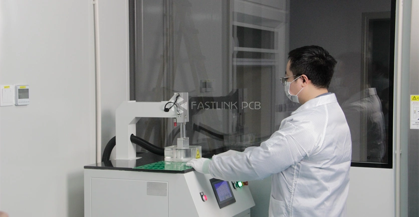
① Measurement Methodology (Marble Plate Method)
✓ Equipment Setup
- Granite surface plate (Grade AA, flatness ≤0.001mm/m²)
- Height gauge (resolution 0.001mm)
✓ Procedure
- Place PCB face-up on marble
- Measure maximum gap (center arch height)
- Record PCB diagonal length (corner-to-corner)
✓ Calculation

② Warpage Tolerance Standards
- Standard PCB: ≤0.75%
- HDI/Rigid-Flex: ≤0.50%
- Customer Specified
Step 9: Digital Quality Management System
① Automated Quality Reporting
All inspection data is automatically logged into Fastlink’s MES in real-time
The system tracks and categorizes defects by:
- Production batch
- PCB type (bulk orders vs prototypes)
- Failure mode (warpage, hole tolerance, etc.)
② Rapid Response Protocol
- Engineering: Investigates root cause
- Production: Implements line adjustments
- Quality: Verifies corrective actions
Our response protocol requires complete root cause analysis and process improvements within 24 hours to prevent recurrence of the same issues.
Final Thoughts
In PCB manufacturing, Final Quality Control (FQC) serves as the critical safeguard to achieve true “zero defect” output from design through delivery. Fastlink has multidimensional system covers all critical quality checkpoints:
- Cleanliness Verification – Particulate and contamination control
- Functional Testing – Electrical performance validation
- Visual Inspection – Surface defect detection
- Dimensional Analysis – Precision measurement verification
This integrated approach ensures consistent quality outcomes while supporting continuous process improvement throughout the manufacturing lifecycle.