- +86-0755-23597570-6067 Mon-Sun 0. 00-23. 59

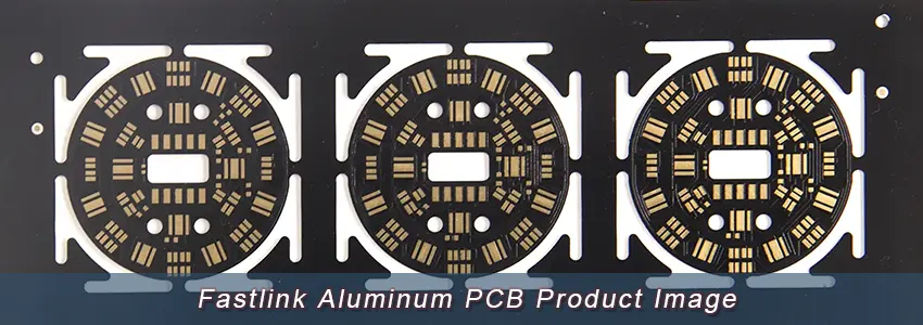
Aluminum PCBs are a subset of Insulated Metal Substrate (IMS) PCBs and stand as one of the most prevalent types of Metal Core PCBs (MCPCB) in today’s electronics industry. At Fastlink, we harness a comprehensive range of high-performance substrates to craft these aluminum PCBs, ensuring a reliable manufacturing and assembly service tailored to your needs, be it for prototyping or large-scale production. Our end-to-end aluminum PCB fabrication capabilities, coupled with complimentary DFM (Design for Manufacturability) checks, empower you to get quality aluminum circuit boards without compromising your budget.
An aluminum PCB is a type of metal core PCB characterized by its metal-based copper clad laminate, which possesses significant heat dissipation capabilities. Often referred to by various names such as aluminum circuit boards, MCPCB (Metal Clad Printed Circuit Board), IMS (Insulated Metal Substrate), aluminum substrate PCB, and aluminum core PCB, they all essentially denote the same type of PCB. Of all the metal core PCBs available, the Aluminum PCB is the most prevalent. The foundational material of this PCB consists of an aluminum core coupled with an insulating layer. This combination effectively dissipates heat, thereby cooling the components and extending their lifespan. Currently, Aluminum PCBs are regarded as the preferred solution for high-power LED applications, including LED street lighting, automobile headlights, and LED high bay lights, among others.

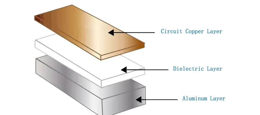
● This is the foundation of the Aluminum PCB.
● It provides structural rigidity, but more importantly, it’s an excellent conductor of heat, making it ideal for applications that generate a lot of heat.
● The thickness of this layer can vary depending on the application, but it’s typically between 0.8mm to 3mm.
● Positioned directly on top of the aluminum base, this layer acts as an insulator.
● It provides electrical isolation between the aluminum base and the copper circuit layer, ensuring that there’s no electrical shorting.
● This layer also plays a crucial role in heat dissipation. It’s typically made of a material with good thermal conductivity, allowing heat to pass through it and into the aluminum base layer where it can be dissipated.
● The thickness of the dielectric layer is usually between 50μm to 200μm.
● This is where the actual circuitry of the PCB is located.
● It’s a thin layer of copper foil that’s laminated onto the dielectric layer.
● The thickness of this layer can vary, but it’s typically between 1oz to 10oz (35μm to 350μm).
● Circuit patterns are etched onto this layer, forming the pathways for electrical currents.
● This is an insulating protective layer applied over the copper circuit layer.
● It’s typically green, but can come in other colors like blue, red, or black.
● The solder mask prevents accidental contact or bridging between solder points during the soldering process. It also protects the copper from environmental factors that could lead to corrosion.
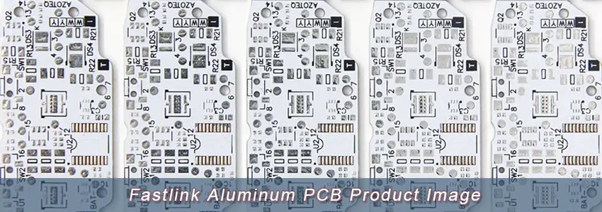
● This is the topmost layer of the PCB.
● It contains markings, symbols, and labels that provide information about the board, such as component designations, test points, and polarity indicators.
● It’s typically white, but other colors can be used.
● To protect the exposed copper circuitry and improve its solderability, a surface finish is applied.
● Common finishes include HASL (Hot Air Solder Leveling), ENIG (Electroless Nickel Immersion Gold), and OSP (Organic Solderability Preservatives).
The combination of these layers gives Aluminum PCBs their unique ability to manage heat effectively. They’re especially useful in high-power applications where traditional PCBs might fail due to excessive heat.

Aluminum PCBs, due to their versatility and heat dissipation capabilities, come in various types to cater to different applications.
Single-layer Aluminum PCBs consist of a single layer of copper conductor, laminated on an aluminum substrate. They are the most basic type of Aluminum PCB and are commonly used in applications that require efficient heat dissipation. Single-layer Aluminum PCBs are suitable for simple circuit designs and low-cost applications.
Double-layer Aluminum PCBs consist of two layers of copper conductor, separated by a dielectric layer, and laminated on an aluminum substrate. The copper layers provide increased routing flexibility and allow for more complex circuit designs compared to single-layer boards. Double-layer Aluminum PCBs are commonly used in applications that require moderate circuit complexity and improved electrical performance.
Multilayer Aluminum PCBs consist of three or more layers of copper conductor, separated by multiple dielectric layers, and laminated on an aluminum substrate. These boards offer the highest level of design flexibility and are suitable for complex circuit designs, high-density interconnections, and advanced electronic applications. Multilayer Aluminum PCBs are used in industries such as telecommunications, aerospace, and high-speed computing.
Hybrid Aluminum PCBs combine aluminum and FR4 materials to leverage the advantages of both. These boards typically have an aluminum core layer sandwiched between FR4 layers. The FR4 layers provide additional mechanical support, while the aluminum core offers excellent heat dissipation. Hybrid Aluminum PCBs are commonly used in applications where a balance between heat dissipation and mechanical strength is required.
High-Frequency Aluminum PCBs are designed specifically for applications that require high-speed signal transmission and minimal signal loss. These boards utilize specialized high-frequency materials, such as PTFE (Polytetrafluoroethylene) or ceramic-filled PTFE, combined with an aluminum core. High-Frequency Aluminum PCBs are commonly used in RF/microwave communication systems, radar systems, and high-speed digital devices.
While not exclusively aluminum-based, Metal Core PCBs deserve mention as they utilize a metal core, which can include aluminum. MCPCBs are designed with a metal base layer (typically aluminum, copper, or steel) and are known for their excellent thermal conductivity and heat dissipation properties. MCPCBs find applications in high-power LED lighting, automotive electronics, power supplies, and other heat-sensitive electronic devices.
1. Material Selection: The primary material for Aluminum PCBs is an aluminum alloy, which acts as the base. This is paired with a thermally insulating layer and then a copper foil. The type of aluminum, insulating material, and copper thickness can vary based on the application.
2. Lamination: The layers are laminated together using heat and pressure. This ensures that the copper foil adheres well to the insulating layer, which in turn is bonded securely to the aluminum base.
3. Circuit Pattern Printing: Once laminated, the desired circuit pattern is printed onto the copper foil using a special ink. This ink acts as a protective barrier in the subsequent etching process.
4. Etching: The board is then subjected to an etching solution. This solution removes the exposed copper, leaving behind only the circuit pattern protected by the ink.
5. Drilling: Holes are drilled into the PCB for component leads or vias. This is done using precise CNC machines to ensure accuracy.
6. Surface Finish: To protect the exposed copper circuitry and improve solderability, a surface finish is applied. Common finishes include HASL (Hot Air Solder Leveling), ENIG (Electroless Nickel Immersion Gold), and OSP (Organic Solderability Preservatives).
7. Solder Mask Application: A solder mask is applied over the circuitry, leaving openings only where soldering will occur. This mask prevents accidental solder bridging during assembly.
8. Silkscreen Printing: For ease of assembly, reference designators and other important information are printed onto the PCB using ink.
9. Testing: Before shipping, the PCBs undergo electrical testing to ensure there are no shorts or open circuits.
10. Cutting and Profiling: The PCBs are then cut from the larger panel and profiled to the desired shape.
11. Final Inspection: A thorough visual inspection is done to ensure the PCB meets all quality standards.
Of course, this is a general overview, and specific processes will vary depending on the manufacturer and the intended application of the PCB.

Aluminum PCBs, while offering numerous advantages especially in terms of heat dissipation, also present unique challenges during the assembly process. Here are some of the key challenges faced during Aluminum PCB assembly:
While Aluminum PCBs are designed for better heat dissipation, this very property can pose challenges during soldering. The rapid heat dissipation can make it difficult to maintain the required temperature for effective soldering, potentially leading to cold solder joints.
Due to the rigidity of Aluminum PCBs, there’s less flexibility in component placement. This can make it challenging to place components in tight or intricate designs.
The thermal properties of Aluminum PCBs can affect the consistency of solder paste application. Ensuring a uniform solder paste deposition becomes crucial to prevent soldering defects.
Aluminum PCBs are more rigid than traditional fiberglass PCBs. This rigidity can introduce mechanical stress during assembly, especially when mounting heavy components, potentially leading to board warping or cracking.
Drilling through Aluminum requires specialized drill bits and techniques. There’s a higher risk of tool wear and breakage, which can increase manufacturing costs.
The dielectric layer in Aluminum PCBs, which provides electrical insulation, can sometimes be a source of concern. If this layer is not uniform or has imperfections, it can lead to electrical shorts or reduced thermal performance.
Not all surface finishes are suitable for Aluminum PCBs. Some finishes might not adhere well to the aluminum substrate, leading to potential reliability issues.
Aluminum PCBs are not suitable for applications that require flexible circuits. Their rigidity can be a limitation in designs that need some degree of flexibility.
While Aluminum PCBs can be cost-effective for specific applications, the specialized manufacturing processes and materials can make them more expensive than traditional PCBs in certain scenarios.
Aluminum PCBs can be more susceptible to ESD damage. Proper handling and ESD protection measures are crucial during the assembly process.
Despite these challenges, the benefits of Aluminum PCBs, especially in high-power and high-temperature applications, often outweigh the drawbacks. Proper design considerations, specialized equipment, and experienced assembly technicians can mitigate many of these challenges.
Fastlink knows that thermal conductivity is one of the important characteristics. We procure high-quality raw materials from premier suppliers, including 6061T6, 5052H34, R-0710, and R-0771. Our aluminum PCBs are produced under a rigorously monitored manufacturing process.
We have dedicated manufacturing facilities in Shenzhen, China, for metal core boards. These facilities handle both low and high-volume Aluminum PCB production, with specialized lines dedicated to rapid-turnaround prototyping.
| Specifications | Aluminum PCB Capabilities |
| Layer | 1-6 Layers |
| Build Time | 1 -4 Weeks |
| Aluminum PCB Types | Single-sided, Double-sided, Multilayer |
| Quality Level | IPC-A-600 Class 3/2 |
| Thermal Conductivity | 1W/mK to 9W/mK |
| Aluminum PCB Substrate Material | 3003 (pure aluminum) 5052 (Al-Mg alloy) 6061 (Al-Mg-Si alloy) 1100 (pure aluminum) |
| Dielectric Layer Material | Polymer Filled With Ceramic |
| Copper Thickness | 1OZ to 8OZ (35μm to 280μm) |
| Manufacturing Condition | Full-line operation; Production Machines And Equipment Specialized For Aluminum PCBs |
| Surface Finish | ENIG, OSP, HASL, Immersion Silver, Immersion Gold |
We are duly certified with the following accreditations:
● IATF 16949:2016
● ISO 9001:2015
● ISO14001:2015
● ISO13485:2016
● UL
Furthermore, all our products adhere to the IPC & ROHS Standards. It is our continuous endeavor to produce premium quality PCB products.
