- +86-0755-23597570-6067 Mon-Sun 0. 00-23. 59

Electronic devices permeate modern life, encompassing a wide range of products from mobile phones, computers, and gaming consoles to essential home appliances like refrigerators and TVs. These devices greatly enhance the convenience of daily living. Their widespread availability and functionality largely depend on the process of electronic assembly.
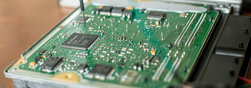
Electronic assembly is the intricate process of placing and connecting various electronic components onto a PCB. This intricate dance of components and connections transforms bare boards into functional modules, known as PCBAs. These PCBAs can then be used to create finished products or serve as building blocks for larger systems.
One of our main specialties is electronic assembly services. We leverage both Surface Mount Technology (SMT) and Through-Hole Technology (THT) to meet the diverse needs of our clients. Additionally, we offer valuable add-on services like conformal coating, rigorous testing, and potting.
Electronics manufacturing involves a systematic multi-stage process that transforms design concepts into tangible electronic products. This process encompasses key stages such as design, component sourcing, assembly, testing, enclosure manufacturing, quality control, and packaging. Each stage plays a pivotal role in ensuring the final product adheres to both design specifications and quality standards.
In this initial phase, the concept for the electronic product is developed. This involves detailed circuit design, selection of components, and software development if needed. Design engineers use various tools like CAD for layout and simulation. After the design phase, a prototype is created. Prototyping is crucial for testing the design’s feasibility, identifying potential issues, and refining the product before mass production. It’s a iterative process, often involving multiple prototype versions.
With a finalized design, sourcing the right components is critical. Electronic assembly manufacturers will consider cost, availability, and performance specifications. Collaborations with multiple suppliers are common to ensure a steady supply of components like semiconductors, resistors, capacitors, and connectors. This stage also includes evaluating the quality and reliability of the components, as they directly affect the final product’s performance.
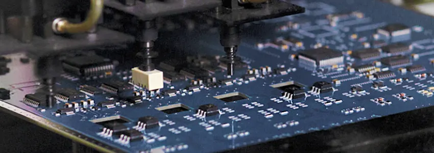
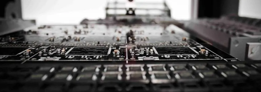
The heart of most electronic products is the PCB. In this stage, the PCB is fabricated based on the design specifications. Then, components are mounted using techniques like Surface Mount Technology and Through-Hole Mounting. Automated machines place tiny components with high precision, and soldering is done either through reflow or wave soldering processes. Inspection methods like Automated Optical Inspection are used to ensure assembly accuracy.
Testing is critical to ensure the product meets functional, performance, and safety standards. This includes functional tests to verify the product operates as intended, environmental tests to ensure durability under various conditions, and reliability tests for long-term performance. Advanced testing methods like In-Circuit Testing (ICT) and Functional Circuit Testing (FCT) are employed.
The enclosure not only protects the internal components but also contributes to the product’s aesthetic and ergonomic appeal. Materials like plastics, metals, or composites are chosen based on durability, weight, and cost. Manufacturing methods can vary from injection molding for plastic to CNC machining for metals. The design of the enclosure also takes into account factors like heat dissipation, user interface, and compliance with regulatory standards.
In this stage, the PCB is integrated into the enclosure, along with other elements like displays, buttons, and connectors. This process might involve manual assembly lines or automated processes, depending on the product complexity. Cable routing, screwing, and final soldering are part of this phase, ensuring all components are securely placed and connected.
Quality control is integral to every stage of manufacturing. It involves a series of inspections, testing, and reviews to ensure that each product adheres to the set standards and specifications. Quality control mechanisms include visual inspections, electrical testing, and performance checks. Any issues identified are addressed to prevent defects in the final product.

The electronics assembly process, also known as PCB Assembly, is a detailed, multi-stage operation that turns bare circuit boards into fully functional electronic devices. It involves various stages, each playing a crucial role in ensuring the final product’s quality, reliability, and functionality. Here’s a detailed breakdown of the key steps:
The process starts with design engineers creating a schematic diagram of the electronic circuit using specialized software. This schematic is then transformed into a physical layout on the PCB, detailing component placement and connections. During this stage, the design undergoes thorough reviews for manufacturability and testability (DFM and DFT), allowing experts to pinpoint and rectify potential production and testing issues.
A comprehensive Bill of Materials (BOM) is compiled, listing all necessary components with their specifications. These components are then sourced from reliable suppliers to ensure they meet quality standards. Efficient inventory management is crucial to keep track of these components and guarantee their availability during assembly.
This phase includes applying solder paste to the PCB using a stencil, followed by precise placement of components via automated machines. The PCB then undergoes soldering through reflow or wave soldering techniques. Post-soldering, Automated Optical Inspection (AOI) checks for any assembly errors like misalignment or soldering issues.
For components with leads, they are inserted into the PCB’s holes, either manually or automatically. The PCB is then passed through a wave soldering process. Some components may also require hand soldering for more precise or delicate connections.
After assembly, the PCB is thoroughly cleaned to eliminate any residual flux or contaminants that might affect its performance.
Rigorous testing is conducted, including In-Circuit Testing (ICT) for component and connection functionality, Functional Testing for overall performance, and Automated X-ray Inspection (AXI) to detect hidden defects.
The PCB is housed in a specially designed enclosure that provides protection, functionality, and aesthetic value. After enclosure assembly, the product is packaged for safe transportation and storage.
Throughout the assembly process, stringent quality control measures are enforced to ensure consistency and adherence to standards. Detailed documentation is maintained for traceability and reference, ensuring a high level of quality and accountability in the manufacturing process.
Achieving a successful PCB assembly process depends on well-informed decisions at the design stage. This requires careful consideration of three key factors: component selection, soldering type, and component placement.
● Assemblers choose components based on the circuit schematic, focusing on their values and characteristics.
● Surface Mount Technology (SMT) components are preferred for their compactness and efficiency.
● Through-Hole Technology (THT) components are used when SMT alternatives are not available.
● Using similar package types for components is recommended to streamline assembly and improve PCB design and functionality.
● The soldering technique must align with the component types used in the PCBA.
● Reflow soldering is typically unsuitable for THT-dominated boards, where wave soldering is more appropriate.
● Manual soldering is reserved for instances where selective or wave soldering is impractical for certain THT components.
● The choice of soldering method greatly affects the PCB’s quality, durability, and reliability.
● Components can be placed manually or via automated processes.
● Proper spacing and orientation of parts are crucial to avoid interference, overheating, and malfunctions.
● Automated placement suits high-volume production but requires precise setup, while manual placement offers flexibility but is slower and more error-prone.
● The method chosen depends on the board’s complexity, production volume, and required precision.
Seeking a reliable partner for your upcoming PCB assembly project? Fastlink is your ideal choice. We provide a diverse range of electronic assembly services, such as cable and harness assembly, box build assembly, electro-mechanical assembly, and LED PCB assembly. Our use of industry-leading equipment and cutting-edge technology enables us to offer rapid product turnaround times. Crucially, our comprehensive in-house testing services ensure the high quality of our products. These services include first article inspection, automatic x-ray inspection, and automated optical inspection.

We handle projects of all sizes and complexities, regardless of product purpose or component diversity. Our advanced infrastructure, combined with extensive production knowledge and efficient supply chain management, allows us to tailor the manufacturing process to your exact needs.
For products requiring additional protection against harsh environments, Fastlink offers conformal coating and potting services. These methods, especially beneficial for electronics exposed to extreme elements, safeguard printed circuit boards from moisture, chemicals, and temperature fluctuations, preventing corrosion and ensuring optimal performance.
By choosing Fastlink for PCB assembly, you gain access to stringent quality control procedures. We utilize cutting-edge X-ray and inline 3D AOI & 3D SPI tools, alongside comprehensive functional, environmental, safety, and in-circuit testing, guaranteeing finished products meet your precise specifications.
Our goal is to execute assembly in line with your specifications, while also enhancing the manufacturing process wherever feasible. Our effective supply chain management, seamlessly integrated with our ERP system and production equipment, ensures a high rate of on-time delivery. This integration aids in streamlining procurement, warehousing, and manufacturing operations, ultimately reducing overall costs.
Fastlink holds crucial certifications for manufacturing electronic equipment, including the ISO 13485 standard for medical devices. Our unique manufacturing execution system (MES) further enhances production traceability, providing you with complete confidence in the quality and consistency of our services.
We have adopted Lean Manufacturing across all our production areas, ensuring high repeatability and standardization in our processes. Consequently, you can trust that electronics assembly at Fastlink consistently adheres to the highest quality standards.
PCB assembly demands precision and meticulous attention to detail. Trusting an experienced professional ensures your project receives the expertise it deserves.
Ready to discuss your electronic assembly needs? Let’s connect!